US 12,088,780 B2
Imaging apparatus and image sensor array
Tomohiro Yamazaki, Kanagawa (JP)
Assigned to SONY SEMICONDUCTOR SOLUTIONS CORPORATION, Kanagawa (JP)
Filed by Sony Semiconductor Solutions Corporation, Kanagawa (JP)
Filed on Jul. 3, 2023, as Appl. No. 18/346,390.
Application 18/346,390 is a continuation of application No. 17/382,058, filed on Jul. 21, 2021, granted, now 11,736,676.
Application 17/382,058 is a continuation of application No. 16/939,699, filed on Jul. 27, 2020, granted, now 11,082,680, issued on Aug. 3, 2021.
Application 16/939,699 is a continuation of application No. 16/565,609, filed on Sep. 10, 2019, granted, now 10,924,723, issued on Feb. 16, 2021.
Application 16/565,609 is a continuation of application No. 16/161,332, filed on Oct. 16, 2018, granted, now 10,425,632, issued on Sep. 24, 2019.
Application 16/161,332 is a continuation of application No. 15/015,427, filed on Feb. 4, 2016, granted, now 10,129,531, issued on Nov. 13, 2018.
Application 15/015,427 is a continuation of application No. 13/771,865, filed on Feb. 20, 2013, granted, now 9,294,756, issued on Mar. 22, 2016.
Claims priority of application No. 2012-034974 (JP), filed on Feb. 21, 2012.
Prior Publication US 2023/0353718 A1, Nov. 2, 2023
Int. Cl. H04N 5/335 (2011.01); H01L 27/146 (2006.01); H04N 13/218 (2018.01); H04N 13/239 (2018.01); H04N 13/257 (2018.01); H04N 25/13 (2023.01); H04N 25/70 (2023.01); H04N 25/702 (2023.01)
CPC H04N 13/239 (2018.05) [H01L 27/14621 (2013.01); H01L 27/14623 (2013.01); H01L 27/14627 (2013.01); H04N 13/218 (2018.05); H04N 13/257 (2018.05); H04N 25/134 (2023.01); H04N 25/70 (2023.01); H04N 25/702 (2023.01)] 8 Claims
OG exemplary drawing
 
1. An imaging apparatus including:
(A) an imaging lens; and
(B) an image sensor array in which a plurality of image sensor units are arrayed, wherein,
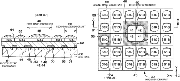
each image sensor unit includes a single microlens and a plurality of image sensors overlaid by the single microlens,
for each image sensor unit, light passing through the imaging lens and reaching the image sensor unit passes through the microlens and forms an image on the plurality of image sensors of the image sensor unit,
in plan view, an inter-unit light shielding layer is formed between the image sensors of different image sensor units, and
for each image sensor unit, a light shielding layer is not formed between the image sensors of the image sensor unit.