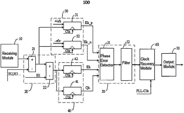
| CPC H04L 7/0058 (2013.01) [H03L 7/0807 (2013.01); H03L 7/085 (2013.01)] | 7 Claims |

|
1. A clock and data recovery circuit comprising:
a receiving module for receiving an analog signal;
a first equalization module connected to the receiving module, the first equalization module comprising a first totalizer for receiving the analog signal and a first equalization coefficient and generating a first superimposed signal, and a second totalizer for receiving the first superimposed signal and a second equalization coefficient and generating a second superimposed signal;
a first sampling module connected to an output end of the first totalizer, the first sampling module comprising a first edge sampler for sampling the first superimposed signal and adjusting a phase of a sampling result with a positive bias voltage to generate a first sampling data and a second edge sampler for sampling the first superimposed signal and adjusting a phase of a sampling result with a negative bias voltage to generate a second sampling data, which are connected to the output end of the first totalizer respectively;
a second sampling module connected to an output end of the second totalizer for sampling the second superimposed signal;
a data processing module connected to both the first sampling module and the second sampling module, the data processing module performing phase error detection according to the first sampling data, the second sampling data and a sampling results of the second sampling module;
a clock recovery module connected to the data processing module, the clock recovery module receiving a clock signal and making a phase adjustment for the clock signal according to a phase error detection result, so as to generate a clock information corresponding to the phase according to a phase adjustment result; and
an output module for outputting the clock information connected to the clock recovery module;
the second sampling module further comprises a data sampler and a third edge sampler respectively connected to the output end of the second totalizer, the third edge sampler sampling the second superimposed signal and generating a third sampling data, and the data sampler sampling the second superimposed signal and generating a fourth sampling data;
the data processing module further comprises a phase error detector connected to an output end of the first edge sampler, an output end of the second edge sampler, an output end of the data sampler and an output end of the third edge sampler, and a filter connected to the phase error detector; and wherein the phase error detector obtains a first error value according to the first sampling data and the second sampling data, obtains a second error value according to the third sampling data and the fourth sampling data, obtains a phase error by summing the first error value and the second error value, and the filter performs digital filtering processing on the phase error.
|