| CPC H03K 19/20 (2013.01) [G06F 1/06 (2013.01); H03K 3/037 (2013.01)] | 20 Claims |

|
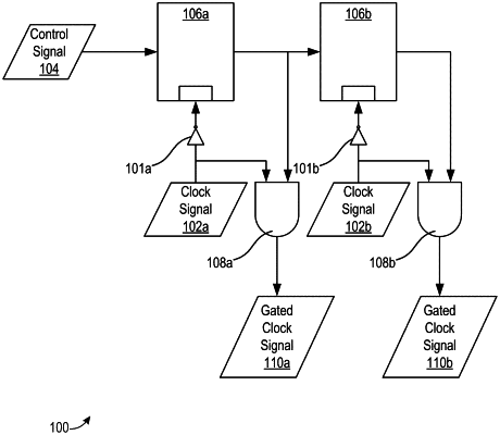
1. A clock circuit for clock gating using a cascaded clock gating control signal, comprising:
a first B-latch accepting, as input, a clock gating control signal and enabled by a first clock signal of a multiphase clock;
a second B-latch accepting, as input, an output from the first B-latch and enabled by a second clock signal of the multiphase clock instead of the first clock signal of the multiphase clock, wherein the output from the first B-latch varies based on the first clock signal to one of a value latched by the first B-latch or the input of the first B-latch and an output from the second B-latch varies based on the second clock signal to either a value latched by the second B-latch or the input of the second B-latch:
a first logic outputting, based on the first B-latch, a first gated clock signal; and
a second logic outputting, based on the second B-latch, a second gated clock signal.
|