| CPC H03K 19/0185 (2013.01) [G05F 1/56 (2013.01); H04L 25/0272 (2013.01); H04L 25/028 (2013.01)] | 16 Claims |

|
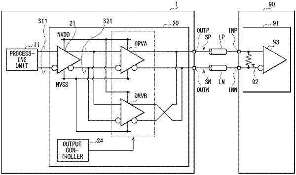
1. A semiconductor device, comprising:
a first output terminal and a second output terminal;
a plurality of first drivers, wherein
each of the plurality of first drivers includes:
a first positive terminal coupled to the first output terminal; and
a first negative terminal coupled to the second output terminal,
at least one driver of the plurality of first drivers is configured to output a first differential signal from the first positive terminal and the first negative terminal, and
the first differential signal corresponds to a first signal;
a plurality of second drivers, wherein
each of the plurality of second drivers includes:
a second positive terminal coupled to the second output terminal;
a second negative terminal coupled to the first output terminal,
at least one driver of the plurality of second drivers is configured to output a second differential signal from the second positive terminal and the second negative terminal, and
the second differential signal corresponds to the first signal; and
a controller configured to set a first number of drivers to be operated out of the plurality of first drivers and a second number of drivers to be operated out of the plurality of second drivers.
|