| CPC H03K 19/0005 (2013.01) [G06F 3/0604 (2013.01); G06F 3/061 (2013.01); G11C 7/1051 (2013.01); G11C 7/1084 (2013.01); H03K 19/017545 (2013.01); H03K 19/01825 (2013.01)] | 20 Claims |

|
1. A memory device, comprising:
a first on-die termination circuit connected to a data pin for transmitting or receiving a data signal and, when enabled, the first on-die termination circuit is configured to provide a first termination resistance to a signal line connected to the data pin;
a second on-die termination circuit connected to a read data strobe pin for transmitting or receiving a read data strobe signal and, when enabled, the second on-die termination circuit is configured to provide a second termination resistance to a signal line connected to the read data strobe pin; and
an on-die termination control circuit configured to independently control an enable timing and a disable timing of the first on-die termination circuit and an enable timing and a disable timing of the second on-die termination circuit,
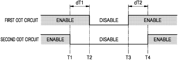
wherein in response to the memory device receiving a read command from a memory controller at a first time point, the on-die termination control circuit is configured to control the second on-die termination circuit in an enable state to be disabled after a first time period from the first time point, control the first on-die termination circuit in an enable state to be disabled after a second time period from the first time point, control the first on-die termination circuit in the disable state to be enabled after a third time period from the first time point, and control the second on-die termination circuit in the disable state to be enabled after a fourth time period from the first time point, and
wherein the first time period is shorter than the second time period, the second time period is shorter than the third time period, and the third time period is shorter than the fourth time period.
|