| CPC H03K 17/063 (2013.01) [H03K 17/04123 (2013.01); H03K 17/165 (2013.01); H03K 2217/0063 (2013.01); H03K 2217/0072 (2013.01)] | 20 Claims |

|
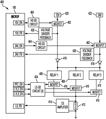
1. A discrete relay driver circuit comprising:
a first high side gate drive circuit configured to drive a first high side metal-oxide-semiconductor field-effect transistor (MOSFET) based on a first voltage enable signal;
a second high side gate drive circuit configured to drive a second high side MOSFET based on a second voltage enable signal;
a first resistor divider configured to sense voltage from the first high side MOSFET;
a second resistor divider configured to sense voltage from the second high side MOSFET;
a first low side gate driver circuit configured to drive a first low side MOSFET based on a power factor correction enable signal;
a second low side gate driver circuit configured to drive a second low side MOSFET based on a first low side enable signal; and
a third low side gate driver circuit configured to drive a third low side MOSFET based on a second low side enable signal.
|