| CPC H03H 3/08 (2013.01) [C23C 14/0641 (2013.01); C23C 14/0652 (2013.01); C23C 14/10 (2013.01); C23C 14/48 (2013.01); C23C 14/5873 (2013.01); C23C 16/24 (2013.01); C23C 16/34 (2013.01); C23C 16/345 (2013.01); C23C 16/401 (2013.01); C23C 16/56 (2013.01)] | 18 Claims |

|
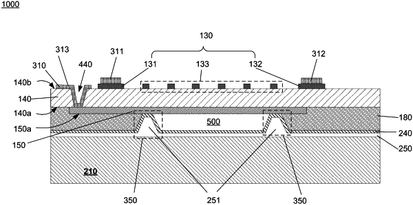
1. A fabrication method of a surface acoustic wave (SAW) filter, comprising:
obtaining a piezoelectric substrate;
forming a back electrode on a first portion of the piezoelectric substrate;
forming a first dielectric layer on the first portion of the piezoelectric substrate, covering the back electrode;
forming a trench in the first dielectric layer and exposing a portion of the back electrode, the trench surrounding a portion of the first dielectric layer;
forming a second dielectric layer on the first dielectric layer and covering sidewalls and a bottom of the trench;
forming a third dielectric layer on the second dielectric layer, the third dielectric layer filling in the trench;
bonding a bottom substrate to the third dielectric layer;
removing a second portion of the piezoelectric substrate and leaving the first portion of the piezoelectric substrate, the first portion of the piezoelectric substrate constituting a piezoelectric layer;
forming an interdigital transducer (IDT) on the piezoelectric layer; and
etching and releasing the portion of the first dielectric layer surrounded by the trench to form a cavity below the back electrode.
|
|
10. A fabrication method of a surface acoustic wave (SAW) filter, comprising:
obtaining a piezoelectric substrate;
forming an interdigital transducer (IDT) on a first portion of the piezoelectric substrate;
forming a first dielectric layer on the first portion of the piezoelectric substrate, covering the IDT;
forming a trench in the first dielectric layer and exposing a portion of the first portion of the piezoelectric substrate, the trench surrounding a portion of the first dielectric layer that covers an interdigital portion of the IDT;
forming a second dielectric layer on the first dielectric layer and covering sidewalls and a bottom of the trench;
forming a third dielectric layer on the second dielectric layer, the third dielectric layer filling in the trench;
bonding a bottom substrate to the third dielectric layer;
removing a second portion of the piezoelectric substrate and leaving the first portion of the piezoelectric substrate, the first portion of the piezoelectric substrate constituting a piezoelectric layer;
forming a back electrode on the piezoelectric layer; and
etching and releasing the portion of the first dielectric layer surrounded by the trench to form a cavity below the interdigital portion of the IDT.
|