| CPC H02M 3/158 (2013.01) [H02M 7/4837 (2021.05); H02M 1/0095 (2021.05); H02M 1/32 (2013.01); H02M 1/36 (2013.01); H02M 3/07 (2013.01)] | 14 Claims |

|
13. A boost power conversion circuit control method, applied to a boost power conversion circuit, the boost power conversion circuit comprising:
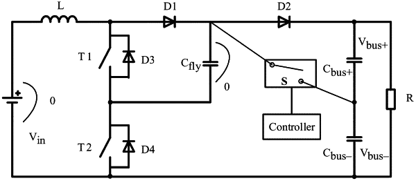
a first switching transistor, a second switching transistor, an inductor, a flying capacitor, a first diode, a second diode, and a voltage control circuit; wherein
the inductor, the first diode, and the second diode are successively connected in series to form a first branch, the first branch is connected in series to an input positive electrode and an input negative electrode of the boost power conversion circuit to form a main circuit, wherein an anode of the first diode is coupled to the input positive electrode of the boost power conversion circuit; the inductor, the first switching transistor, and the second switching transistor are connected in series to form a first closed loop, and the first switching transistor, the second switching transistor, the first diode, and the second diode form a second closed loop; and one end of the flying capacitor is connected to a common point of the first diode and the second diode, and an other end of the flying capacitor is connected to a common point of the first switching transistor and the second switching transistor; and
a first end of the voltage control circuit is connected to a common end of the first diode and the second diode, a second end of the voltage control circuit is connected to a reference point, the reference point is used to provide a clamping potential, and the clamping potential is between a negative bus potential and a positive bus potential; and the voltage control circuit is configured to clamp a voltage of the common point of the first diode and the second diode when a voltage on an input end of the boost power conversion circuit is less than a startup voltage of the boost power conversion circuit,
wherein the voltage control circuit comprises a third closed loop and the third closed loop comprises one of a controllable switching transistor and a compound component to form the third closed loop:
wherein the method comprises:
when a voltage on an input end of the boost power conversion circuit is less than a startup voltage of the boost power conversion circuit, controlling, by the voltage control circuit, a voltage borne by the second diode to be less than a bus voltage of the boost power conversion circuit, wherein the bus voltage is a voltage difference between a positive bus voltage and a negative bus voltage.
|