| CPC H02M 1/088 (2013.01) [H02M 3/07 (2013.01); H03K 17/6871 (2013.01); H03K 2217/0063 (2013.01)] | 19 Claims |

|
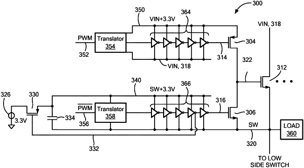
1. A system for driving a plurality of high side NMOS power switches, each coupled between an input voltage and a floating switch node, comprising:
a charge pump configured to generate a boot voltage across a charge pump capacitor; and
a plurality of high side drivers, each configured to generate a power control signal to control a respective high side NMOS power switch and comprising:
a PMOS switch to turn on the high side NMOS power switch;
an NMOS switch to turn off the high side NMOS power switch, wherein the PMOS switch and the NMOS switch are coupled together at a control node at which the power control signal is provided;
a first inverter chain coupled between the boot voltage and the input voltage and configured to generate a first control signal to control the PMOS switch;
a circuit configured to generate an internal boot voltage; and
a second inverter chain coupled between the internal boot voltage and the floating switch node and configured to generate a second control signal to control the NMOS switch.
|