| CPC H01S 5/0281 (2013.01) [H01S 5/18369 (2013.01); H01S 5/343 (2013.01)] | 16 Claims |

|
1. A light emitting element, comprising:
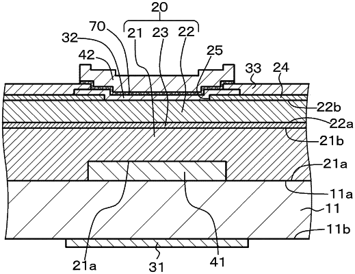
a layered structure that includes:
a first light reflecting layer that includes a first plurality of thin films;
a light emitting structure; and
a second light reflecting layer that includes a second plurality of thin films, wherein
the light emitting structure is between the first light reflecting layer and the second light reflecting layer, and
the light emitting structure includes:
a first compound semiconductor layer on the first light reflecting layer;
an active layer on the first compound semiconductor layer; and
a second compound semiconductor layer on the active layer;
an intermediate layer between the second compound semiconductor layer and the second light reflecting layer; and
an electrode between the intermediate layer and the second compound semiconductor layer, wherein
a first surface of the intermediate layer faces the electrode,
a second surface of the intermediate layer is in contact with the second light reflecting layer, and
a value of a surface roughness of the second surface of the intermediate layer is less than a value of a surface roughness of the first surface of the intermediate layer.
|