| CPC H01Q 21/065 (2013.01) [H01Q 1/243 (2013.01); H01Q 5/25 (2015.01); H01Q 9/045 (2013.01)] | 16 Claims |

|
1. An electronic device comprising:
an antenna structure comprising at least one antenna; and
at least one processor operatively connected with the antenna structure,
wherein the antenna structure includes:
a dielectric substance;
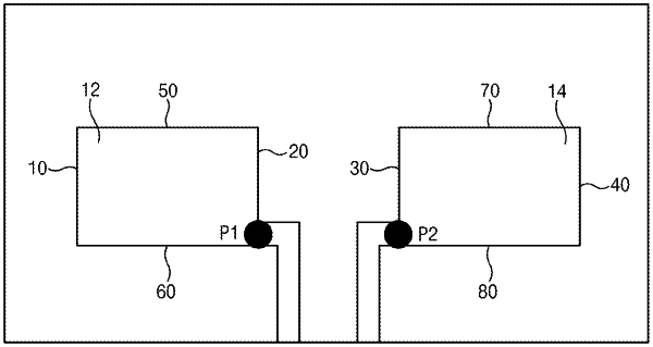
a first conductive patch disposed on the dielectric substance, the first conductive patch including a first edge and a second edge parallel to the first edge;
a first transmission line electrically connected to a first point of the first conductive patch;
a second conductive patch disposed on the dielectric substance and spaced apart from the first conductive patch by a specified distance, the second conductive patch including a third edge at least partially facing the second edge of the first conductive patch and a fourth edge parallel to the third edge;
a second transmission line electrically connected to a second point of the second conductive patch; and
a ground disposed under the dielectric substance,
wherein the at least one processor is configured to: control the electronic device to receive wireless signals of a specified band by supplying power to the first conductive patch and the second conductive patch through the first transmission line and the second transmission line and determine phase difference of arrival (PDOA) between wireless signals received by the first conductive patch and the second conductive patch, and
wherein
the specified distance is less than half of a wavelength of the wireless signals received by the first conductive patch and the second conductive patch, the first point of the first conductive patch is located
on the second edge of the first conductive patch, and the second point of the second conductive patch is located on the third edge of the second conductive patch; or
the specified distance exceeds half of the wavelength of the wireless signals received by the first conductive patch and the second conductive patch, the first point of the first conductive patch is located on the first edge of the first conductive patch, and the second point of the second conductive patch is located on the fourth edge of the second conductive patch.
|