| CPC H01P 5/107 (2013.01) [H05K 1/0225 (2013.01); H05K 1/0246 (2013.01); H05K 1/144 (2013.01); H05K 2201/042 (2013.01); H05K 2201/096 (2013.01); H05K 2201/09609 (2013.01); H05K 2201/10098 (2013.01)] | 9 Claims |

|
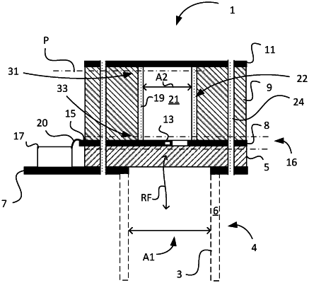
1. A waveguide launch system configured for translating radio frequency signal waves, the waveguide launch system comprising:
a separate waveguide channel of a separate waveguide element having a first cross-section area;
a first printed circuit board lamina comprising an electrically conductive ground member and configured for attachment of the separate waveguide element thereto;
a second printed circuit board lamina comprising an electrically conductive backshort cover configured to reflect the radio frequency signal waves;
a probe member arranged within an interface defined between the first printed circuit board lamina and the second printed circuit board lamina;
an electrical transmission line signal member arranged within said interface and coupled between the probe member and an integrated circuit unit; wherein
a thickness of the second printed circuit board lamina is determined by a material property of the second printed circuit board lamina being permittivity of a PCB material used and by scaling of said thickness when taking into account the wavelength of the radio frequency signal waves, wherein
a thickness of the integrated circuit unit corresponds with a thickness of the first printed circuit board lamina; the waveguide launch system further comprises:
an electrically conductive barrier arrangement extending perpendicular to a plane of the second printed circuit board lamina and extending through the second printed circuit board lamina, wherein the electrically conductive barrier arrangement and the electrically conductive backshort cover form an integrated electrically conductive backshort volume of an integrated backshort having a second cross-section area, which is smaller than the first cross-section area,
wherein
an outer electrically conductive barrier arrangement is configured to at least partially surround the electrically conductive barrier arrangement and the outer electrically conductive barrier arrangement extends perpendicular to the plane and through the first and second printed circuit board lamina.
|