| CPC H01L 31/0203 (2013.01) [H01L 25/167 (2013.01); H01L 33/483 (2013.01)] | 12 Claims |

|
1. An assembly for a semiconductor photonic component, the assembly at least comprising:
a substrate;
at least one semiconductor photonic component mounted to the substrate, said at least one semiconductor photonic component including a photonic active surface element;
an assembly housing for shielding the substrate and the at least one semiconductor photonic component from the environment;
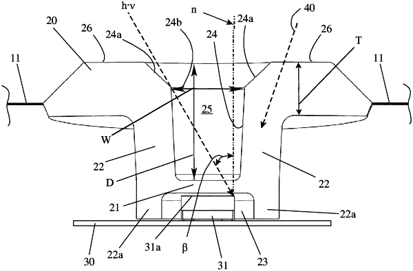
the assembly housing comprises a housing wall part having an exterior surface and being provided with at least one photonic window element facing the photonic active surface element of the at least one semiconductor photonic component, said at least one photonic window element being a bottom wall of a recess in said exterior surface and forming a monolithic part with the housing wall part,
wherein the at least one photonic window element has a thickness which is smaller than a thickness of the housing wall part for having a transmissivity being larger than the transmissivity of the housing wall part, the recess has a side wall at least partly formed by upright housing wall sections and has a depth D which is larger than the thickness T of the housing wall part, and
wherein the housing wall part contains a light absorbing dope and/or light blocking dope.
|