US 12,087,865 B2
Thin film transistor and thin film transistor array panel including the same
Yong Su Lee, Hwaseong-si (KR); Yoon Ho Khang, Yongin-si (KR); Dong Jo Kim, Yongin-si (KR); Hyun Jae Na, Seoul (KR); Sang Ho Park, Suwon-si (KR); Se Hwan Yu, Seoul (KR); Chong Sup Chang, Hwaseong-si (KR); Dae Ho Kim, Daegu (KR); Jae Neung Kim, Seoul (KR); Myoung Geun Cha, Seoul (KR); Sang Gab Kim, Seoul (KR); and Yu-Gwang Jeong, Anyang-si (KR)
Assigned to SAMSUNG DISPLAY CO., LTD., Yongin-si (KR)
Filed by SAMSUNG DISPLAY CO., LTD., Yongin-si (KR)
Filed on Feb. 28, 2023, as Appl. No. 18/176,454.
Application 18/176,454 is a continuation of application No. 17/115,470, filed on Dec. 8, 2020, granted, now 11,594,639.
Application 17/115,470 is a continuation of application No. 16/231,781, filed on Dec. 24, 2018, granted, now 10,861,978, issued on Dec. 8, 2020.
Application 16/231,781 is a continuation of application No. 15/704,063, filed on Sep. 14, 2017, granted, now 10,192,992, issued on Jan. 29, 2019.
Application 15/704,063 is a continuation of application No. 15/194,841, filed on Jun. 28, 2016, granted, now 9,768,309, issued on Sep. 19, 2017.
Application 15/194,841 is a continuation of application No. 14/666,461, filed on Mar. 24, 2015, granted, now 9,379,252, issued on Jun. 28, 2016.
Application 14/666,461 is a continuation of application No. 14/184,361, filed on Feb. 19, 2014, granted, now 8,987,047, issued on Mar. 24, 2015.
Application 14/184,361 is a continuation in part of application No. 13/553,418, filed on Jul. 19, 2012, granted, now 8,664,654, issued on Mar. 4, 2014.
Claims priority of application No. 10-2012-0034099 (KR), filed on Apr. 2, 2012; and application No. 10-2013-0131410 (KR), filed on Oct. 31, 2013.
Prior Publication US 2023/0215954 A1, Jul. 6, 2023
Int. Cl. H01L 27/12 (2006.01); H01L 29/417 (2006.01); H01L 29/66 (2006.01); H01L 29/786 (2006.01); H10K 59/121 (2023.01)
CPC H01L 29/78633 (2013.01) [H01L 27/1225 (2013.01); H01L 27/124 (2013.01); H01L 27/1288 (2013.01); H01L 29/41733 (2013.01); H01L 29/66969 (2013.01); H01L 29/78618 (2013.01); H01L 29/7869 (2013.01); H01L 29/78696 (2013.01); H10K 59/1213 (2023.02)] 23 Claims
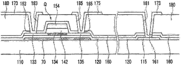
OG exemplary drawing
 
1. A display device, comprising:
a substrate;
a first insulating layer disposed on the substrate;
a light blocking layer disposed between the substrate and the first insulating layer;
a data line disposed between the substrate and the first insulating layer;
a semiconductor layer disposed on the first insulating layer, the semiconductor layer including a first region, a second region, and a channel region between the first region and the second region;
a second insulating layer disposed on the semiconductor layer;
a gate electrode disposed on the second insulating layer;
a third insulating layer disposed on the gate electrode; and
a first electrode disposed on the third insulating layer,
wherein the third insulating layer has a first opening on the first region, and the first electrode is electrically connected to the first region through the first opening.