| CPC H01L 29/786 (2013.01) [H03F 1/565 (2013.01); H03H 7/38 (2013.01); H03H 11/28 (2013.01)] | 7 Claims |

|
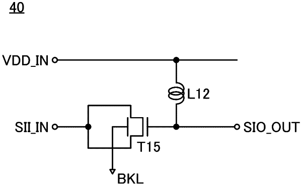
1. An impedance-matching circuit comprising:
a first input terminal configured to input an alternating-current signal;
a second input terminal configured to input a constant potential;
an output terminal;
a transistor comprising a first gate, a second gate, a source and a drain; and
an inductor comprising a first terminal and a second terminal,
wherein one of the source and the drain is electrically connected to the first input terminal,
wherein the first gate of the transistor is electrically connected to the first terminal of the inductor,
wherein the output terminal is electrically connected to the second terminal of the inductor,
wherein the second terminal of the inductor is configured to input a first constant potential,
wherein the transistor comprises an oxide semiconductor, and
wherein the second input terminal is configured to change the constant potential from the first constant potential into a second constant potential.
|