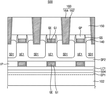
| CPC H01L 29/7856 (2013.01) [H01L 21/845 (2013.01); H01L 27/1211 (2013.01); H01L 29/0653 (2013.01); H01L 29/42376 (2013.01); H01L 29/6653 (2013.01); H01L 29/66553 (2013.01); H01L 29/6681 (2013.01); H01L 29/36 (2013.01)] | 20 Claims |

|
1. A semiconductor device, comprising:
a substrate;
a first semiconductor pattern on the substrate, the first semiconductor pattern including a first part protruding from an upper surface of the substrate and a second part on the first part;
a semiconductor oxide layer between the first part and the second part;
a second semiconductor pattern on the first semiconductor pattern and spaced apart from the first semiconductor pattern in a vertical direction;
a gate electrode covering the second part and surrounding the second semiconductor pattern; and
source/drain patterns on opposite sides of the second semiconductor pattern,
wherein the entire semiconductor oxide layer is vertically overlapped by a lower surface of the second part.
|