| CPC H01L 29/7848 (2013.01) [H01L 29/49 (2013.01); H01L 29/51 (2013.01); H01L 29/66545 (2013.01); H01L 29/66795 (2013.01); H01L 29/7834 (2013.01); H01L 29/7843 (2013.01); H01L 29/785 (2013.01)] | 20 Claims |

|
1. A semiconductor device comprising:
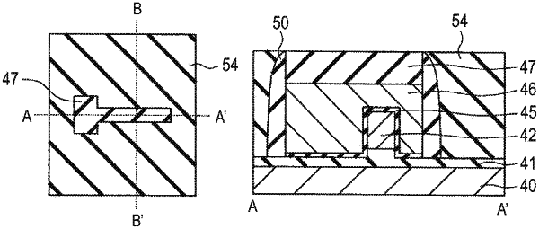
a semiconductor region that extends linearly along a longitudinal direction, a channel region of the semiconductor region is between source/drain regions of the semiconductor region;
a gate electrode that extends linearly along a transverse direction, the transverse direction and the longitudinal direction intersect at the channel region;
an insulating film between the channel region and the gate electrode, the gate electrode is between the insulating film and a first stress application layer;
a buried insulator between a substrate and the semiconductor region along a vertical direction, a second stress application layer extends from a top surface of the buried insulator along the vertical direction; and
respective first and second sidewall insulating films between the first stress application layer and the second stress application layer, the second stress application layer surrounds the semiconductor region and the respective first and second sidewall insulating films,
wherein a lower surface of the buried insulator contacts the substrate, and
a central portion of the buried insulator located between the respective first and second sidewall insulating films and bounded by the channel region extends vertically in the transverse direction such that an upper surface of the central portion of the buried insulator is higher than upper surfaces of the buried insulator outside the channel region,
a lower surface of the respective first and second sidewall insulating films is in direct contact with an upper surface of the buried insulator outside the channel region, and
an upper surface of the central portion of the buried insulator is higher than the lower surface of the respective first and second sidewall insulating films.
|