| CPC H01L 29/7813 (2013.01) [H01L 29/1095 (2013.01); H01L 29/24 (2013.01); H01L 29/41741 (2013.01); H01L 29/8083 (2013.01)] | 6 Claims |

|
1. A trench junction field-effect transistor without using a p-type Ga2O3-based single crystal, comprising:
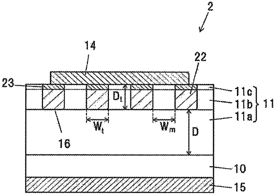
an n-type semiconductor layer comprising an n-type Ga2O3-based single crystal and having a plurality of trenches opening on one surface;
a gate electrode buried in each of the plurality of trenches;
a source electrode connected to a mesa-shaped region between adjacent trenches in the n-type semiconductor layer comprising the n-type Ga2O1-based single crystal; and
a drain electrode directly or indirectly connected to the n-type semiconductor layer comprising the n-type Ga2O3-based single crystal on an opposite side to the source electrode,
wherein the gate electrode is buried in each of the trenches in a state of being prevented from contacting the source electrode by a dielectric film,
wherein the trench junction field-effect transistor does not include a region having a p-type Ga2O3-based single crystal,
wherein the gate electrode comprises a p-type semiconductor, and
wherein the gate electrode comprising the p-type semiconductor and the n-type semiconductor layer comprising the n-type Ga2O3-based single crystal are in contact with each other to form a p-n junction.
|