| CPC H01L 29/7813 (2013.01) [H01L 21/26553 (2013.01); H01L 29/2003 (2013.01); H01L 29/66734 (2013.01)] | 12 Claims |

|
1. A method for manufacturing a vertical UMOSFET device with a high channel mobility, comprising the steps of:
manufacturing an epitaxial structure comprising a substrate;
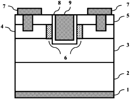
manufacturing a source, a drain and a gate which match the epitaxial structure, wherein the epitaxial structure comprises a first semiconductor, and a second semiconductor and a third semiconductor which are sequentially disposed on the first semiconductor; wherein the first semiconductor is grown on the substrate, wherein the second semiconductor is grown on the first semiconductor, and wherein the third semiconductor is grown on the second semiconductor, wherein a groove structure matching the gate is also disposed in the epitaxial structure, and the groove structure continuously extends into the first semiconductor from a first surface of the epitaxial structure; wherein the first surface of the epitaxial structure is a surface of the third semiconductor facing away from the second semiconductor wherein the manufacturing method also comprises the step of manufacturing a fourth semiconductor in the epitaxial structure; the fourth semiconductor is disposed at least between an inner wall of the groove structure and the second semiconductor, and the fourth semiconductor comprises any one of GaN and InGaN, wherein the step of manufacturing the groove structure is performed after the step of forming the fourth semiconductor,
by processing at least a region of the second semiconductor corresponding to the groove structure and the fourth semiconductor first to convert a composition material of the second semiconductor in the region into a material of the fourth semiconductor, and then processing the groove structure in the epitaxial structure.
|