| CPC H01L 29/7786 (2013.01) [H01L 27/1214 (2013.01); H01L 27/156 (2013.01); H01L 29/66462 (2013.01); H01L 29/778 (2013.01); H01L 27/15 (2013.01)] | 7 Claims |

|
1. A method of manufacturing a semiconductor device, the method comprising:
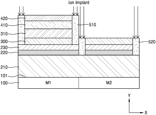
stacking a lower semiconductor layer, an active layer, an upper semiconductor layer, a separation layer, an etch-stop layer, a channel layer, and a channel supply layer on an upper region of a substrate which includes a first region and a second region adjacent to the first region, the first region and the second region being disposed in a first direction parallel to an upper surface of the substrate;
etching a portion of the channel supply layer, a portion of the channel layer, and a portion of the separation layer disposed on the second region, in a second direction perpendicular to the upper surface of the substrate;
performing a high-temperature heat treatment process on the etch-stop layer; and
forming a plurality of first insulating patterns by implanting a first dopant into side surfaces of another portion of the channel supply layer, another portion of the channel layer, another portion of the separation layer, and a portion of the etch-stop layer, which are disposed on the first region, and forming second insulating patterns by implanting a second dopant into side surfaces of another portion of the etch-stop layer, a portion of the upper semiconductor layer, and a portion of the active layer, which are disposed on the second region.
|