| CPC H01L 29/7786 (2013.01) [H01L 29/1075 (2013.01); H01L 29/267 (2013.01); H01L 29/66068 (2013.01); H01L 29/66462 (2013.01); H01L 29/1608 (2013.01); H01L 29/167 (2013.01); H01L 29/2003 (2013.01); H01L 29/205 (2013.01)] | 10 Claims |

|
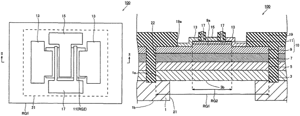
1. A compound semiconductor device comprising:
a Si substrate with a shape that surrounds a hole when viewed in a plane;
a covalent crystal layer formed on a top surface of the Si substrate and covering the hole;
a wide gap semiconductor layer including Ga formed on a top surface side of the crystal layer; and
a first, a second, and a third electrodes formed on a top surface side of the wide gap semiconductor layer, wherein
current flowing between the first electrode and the second electrode can be controlled by voltage applied to the third electrode, and
the Si substrate does not exist in a region that overlaps with the first, second, and third electrodes when viewed from a direction orthogonal to the top surface of the Si substrate,
the compound semiconductor device further comprising
a separation region formed to a depth from the top surface of the wide gap semiconductor layer to a top surface of the Si substrate, wherein the compound semiconductor device is electrically separated from another compound semiconductor device adjacent to the compound semiconductor device by the separation region.
|