| CPC H01L 29/41775 (2013.01) [H01L 21/76897 (2013.01); H01L 29/0847 (2013.01); H01L 29/41791 (2013.01); H01L 29/6681 (2013.01); H01L 29/7851 (2013.01)] | 15 Claims |

|
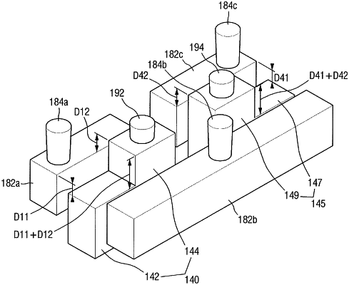
1. A semiconductor device, comprising:
an active pattern on a substrate, the active pattern extending in a first direction;
a gate electrode on the active pattern, a longitudinal direction of the gate electrode extending in a second direction intersecting the first direction, and the gate electrode including a first portion and a second portion arranged adjacent to each other along the second direction;
a source/drain region in the active pattern on a sidewall of the gate electrode;
a source/drain contact connected to the source/drain region; and
a first contact plug connected to the source/drain contact on a sidewall of the first portion of the gate electrode, a portion of the first contact plug not overlapping with the source/drain contact,
wherein a height of a top surface of the first portion of the gate electrode is lower than a height of a top surface of the second portion of the gate electrode, and
wherein a height of a bottom surface of the first contact plug is higher than the height of the top surface of the first portion of the gate electrode.
|