| CPC H01L 29/24 (2013.01) [C03C 17/245 (2013.01); C04B 35/01 (2013.01); C04B 35/453 (2013.01); C04B 35/62218 (2013.01); C23C 14/08 (2013.01); C23C 14/5853 (2013.01); H01L 27/1225 (2013.01); H01L 29/7782 (2013.01); H01L 29/7786 (2013.01); H01L 29/78648 (2013.01); H01L 29/7869 (2013.01); H01L 29/78696 (2013.01); C03C 2217/23 (2013.01); C03C 2218/151 (2013.01); C04B 2235/3217 (2013.01); C04B 2235/3225 (2013.01); C04B 2235/3284 (2013.01); C04B 2235/3286 (2013.01); C04B 2235/3293 (2013.01); C04B 2235/787 (2013.01); C04B 2235/96 (2013.01)] | 12 Claims |

|
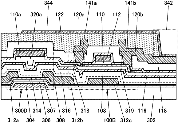
1. A semiconductor device comprising:
a first gate electrode over a substrate;
a first oxide semiconductor film over the first gate electrode;
a first source electrode and a first drain electrode over and in electrical contact with the first oxide semiconductor film;
a first conductive film;
a first insulating film over and in contact with a top surface of the first source electrode, a top surface of the first drain electrode, and a top surface of the first conductive film;
a second oxide semiconductor film over the first insulating film;
a second gate electrode over the second oxide semiconductor film;
a second conductive film;
a second insulating film over and in contact with a top surface of the second gate electrode and a top surface of the second conductive film;
a second source electrode and a second drain electrode over and in electrical contact with the second oxide semiconductor film; and
a pixel electrode over and in electrical contact with one of the second source electrode and the second drain electrode,
wherein the first gate electrode and the second conductive film overlap with each other, and
wherein the first conductive film and the second gate electrode overlap with each other.
|