| CPC H01L 29/0696 (2013.01) [H01L 29/66333 (2013.01); H01L 29/7395 (2013.01)] | 23 Claims |

|
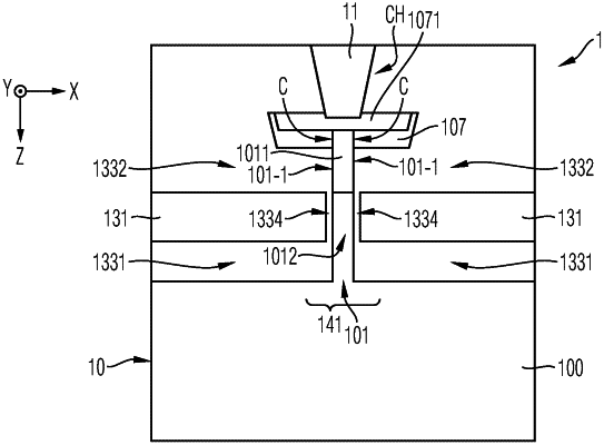
1. A power semiconductor device, comprising
a control cell configured to control a load current and electrically connected to a first load terminal structure of the power semiconductor device on one side and electrically connected to a drift region of the power semiconductor device on another side, the drift region comprising dopants of a first conductivity type,
wherein the control cell comprises:
a mesa extending along a vertical direction and including a contact region having dopants of the first conductivity type or of a second conductivity type complementary to the first conductivity type and electrically connected to the first load terminal structure, and a channel region coupled to the drift region;
a control electrode configured to control a conduction channel in the channel region; and
a contact plug comprising at least one of a doped semiconductive material and metal, and arranged in contact with the contact region,
wherein an electrical connection between the contact region and the first load terminal structure is established by the contact plug,
wherein a portion of the contact plug horizontally projects beyond lateral boundaries of the mesa.
|