| CPC H01L 27/156 (2013.01) [H01L 23/60 (2013.01); H01L 33/483 (2013.01); H01L 33/50 (2013.01)] | 20 Claims |

|
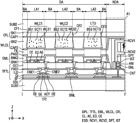
1. A display device comprising:
a first substrate including:
a display area comprising a plurality of pixels; and
a non-display area surrounding the display area;
a thin film transistor layer disposed on the first substrate and comprising a thin film transistor;
a second substrate disposed on the thin film transistor layer and facing the first substrate;
a sealing part disposed between the first substrate and the second substrate in the non-display area, and bonding the first substrate and the second substrate;
a metal line disposed in the non-display area on the thin film transistor layer and overlapping the sealing part; and
an antistatic member comprising:
a support supported by the metal line;
a first receiver protruding from a top portion of the support toward an exterior of the sealing part; and
a second receiver protruding from a bottom portion of the support toward the exterior of the sealing part and facing the first receiver.
|