| CPC H01L 27/15 (2013.01) [H01L 33/382 (2013.01); H01L 33/44 (2013.01); H01L 33/505 (2013.01); H01L 33/58 (2013.01); H01L 33/62 (2013.01); H01L 2933/0016 (2013.01); H01L 2933/0025 (2013.01); H01L 2933/0066 (2013.01)] | 18 Claims |

|
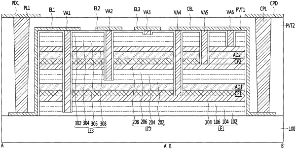
1. A light emitting device comprising:
a substrate having a first region and a second region;
a light emitting stack including vertically stacked semiconductor layers disposed on the first region of the substrate;
at least one pillar including a region disposed on the second region of the substrate and laterally spaced apart from the light emitting stack;
at least one electrode extending from the first region to the second region of the substrate and electrically connecting the light emitting stack to the at least one pillar; and
a passivation layer covering the light emitting stack and the substrate; and
a plurality of pads electrically connected to the at least one pillar, respectively wherein the at least one pillar is connected to the at least one electrode, respectively, and
wherein the passivation layer comprises at least one epoxy resin, epoxy molding compound, or silicone.
|