| CPC H01L 27/14641 (2013.01) [H01L 27/14638 (2013.01)] | 12 Claims |

|
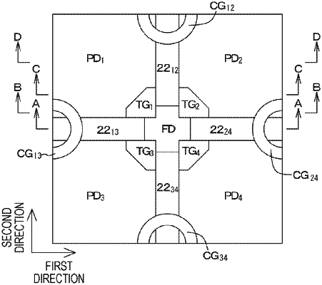
1. An imaging device comprising a plurality of imaging elements, wherein
each of the imaging elements includes:
M×N photoelectric conversion regions arrayed such that M photoelectric conversion regions are arrayed in a first direction and N photoelectric conversion regions are arrayed in a second direction different from the first direction;
a floating diffusion layer shared by the M×N photoelectric conversion regions;
a transfer control electrode that is disposed corresponding to each of the M×N photoelectric conversion regions and transfers charges generated in each of the M×N photoelectric conversion regions to the floating diffusion layer;
(M−1)×N first charge transfer control electrodes that control charge transfer between the M photoelectric conversion regions arrayed in the first direction; and
(N−1)×M second charge transfer control electrodes that control charge transfer between the N photoelectric conversion regions arrayed in the second direction,
in the M photoelectric conversion regions arrayed in the first direction, an m-th first charge transfer control electrode [in which m is any integer of 1 to (M−1)] controls charge transfer between an m-th photoelectric conversion region and an (m+1)-th photoelectric conversion region, and
in the N photoelectric conversion regions arrayed in the second direction, an n-th second charge transfer control electrode [in which n is any integer of 1 to (N−1)] controls charge transfer between an n-th photoelectric conversion region and an (n+1)-th photoelectric conversion region.
|