| CPC H01L 27/14636 (2013.01) [H01L 27/14618 (2013.01)] | 9 Claims |

|
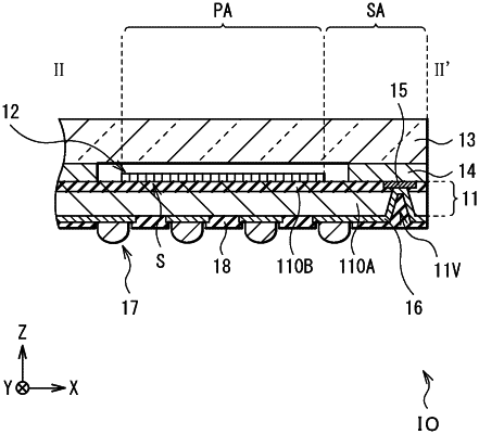
1. An imaging device, comprising:
a pixel area;
a peripheral area that lies outside the pixel area;
a light receiving element in the pixel area;
a circuit board in the pixel area and the peripheral area, wherein
the circuit board includes a semiconductor substrate and a multilayer wiring layer, and
the multilayer wiring layer is between the semiconductor substrate and the light receiving element;
a first wiring line in the multilayer wiring layer, wherein the first wiring line is electrically coupled to the light receiving element;
a second wiring line in the multilayer wiring layer, wherein the second wiring line is electrically coupled to the light receiving element;
a protective member opposed to the circuit board, wherein the protective member and the circuit board sandwich the light receiving element; and
an extended wiring section between the semiconductor substrate and the protective member in the peripheral area, wherein
at least a portion of the extended wiring section includes a wiring layer in a layer in which the second wiring line is provided, and
one end of the extended wiring section is open and another end of the extended wiring section is electrically coupled to the first wiring line.
|