| CPC H01L 27/14616 (2013.01) [H01L 27/14621 (2013.01); H01L 27/14627 (2013.01); H01L 27/14638 (2013.01); H01L 27/14645 (2013.01); H03M 1/56 (2013.01); H04N 25/75 (2023.01); H04N 25/772 (2023.01)] | 20 Claims |

|
1. An image sensor comprising:
a substrate; and
a plurality of pixels disposed in a first direction and a second direction intersecting with the first direction, the first direction and the second direction being parallel to an upper surface of the substrate,
wherein the plurality of pixels includes a plurality of first pixels and a plurality of second pixels and a number of the plurality of second pixels is greater than a number of the plurality of first pixels,
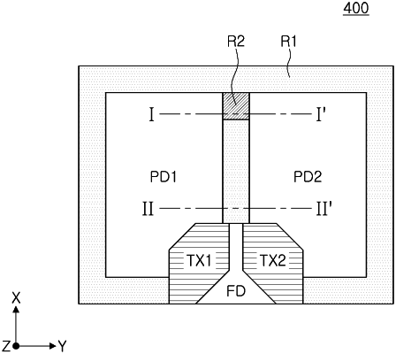
wherein each of the plurality of pixels includes a first photodiode and a second photodiode being adjacent to the first photodiode,
wherein each of the plurality of first pixels includes a well disposed between the first photodiode and the second photodiode and doped with a first conductivity-type impurities, and
wherein each of the plurality of second pixels includes a first well and a second well disposed between the first photodiode and the second photodiode, the first well is doped with the first conductivity-type impurities, and the second well is doped with a second conductivity-type impurities different from the first conductivity-type impurities.
|