| CPC H01L 27/14614 (2013.01) [H01L 27/14643 (2013.01); H01L 27/14689 (2013.01)] | 19 Claims |

|
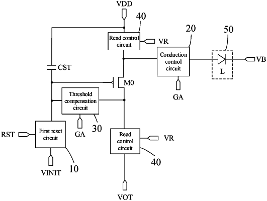
1. A photoelectric conversion circuit, comprising:
a photoelectric conversion device, configured to receive incident light and generate an operating voltage after photoelectric conversion of the incident light;
a driving transistor, configured to generate a detection current according to the operating voltage photoelectrically converted by the photoelectric conversion device;
a first reset circuit, configured to supply a signal of an initialization signal terminal to a gate of the driving transistor in response to a signal of a reset control signal terminal;
a conduction control circuit, configured to conduct the photoelectric conversion device with the driving transistor in response to a signal at a scan signal terminal;
a threshold compensation circuit, configured to conduct the gate of the driving transistor and a second electrode of the driving transistor in response to the signal at the scan signal terminal; and
a read control circuit, configured to conduct a first power supply terminal with a first electrode of the driving transistor and conduct the second electrode of the driving transistor with a read output terminal, in response to a signal of a read control signal terminal.
|