| CPC H01L 27/1461 (2013.01) [G06V 40/1318 (2022.01); H01L 25/18 (2013.01); H01L 27/14612 (2013.01); H01L 27/1463 (2013.01); H01L 27/14692 (2013.01); H01L 27/14625 (2013.01); H01L 27/14636 (2013.01)] | 7 Claims |

|
1. A fingerprint sensor comprising:
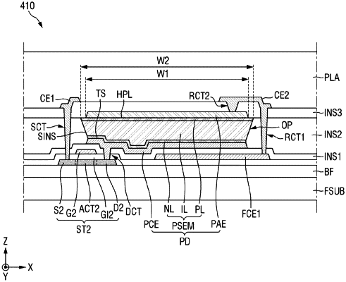
a thin film transistor disposed on a substrate;
a first insulating layer disposed on the thin film transistor;
a first sensing electrode disposed on the first insulating layer and connected to the thin film transistor;
a second insulating layer disposed on the first sensing electrode and including an opening exposing the first sensing electrode;
a sensing semiconductor layer disposed in the opening of the second insulating layer and on the first sensing electrode, and including an N-type semiconductor layer, an I-type semiconductor layer, and a P-type semiconductor layer;
a second sensing electrode disposed on the sensing semiconductor layer;
a first fingerprint capacitor electrode electrically connected to the second sensing electrode;
a first connection electrode connected to the thin film transistor, and extending in a vertical direction with respect to an upper surface of the substrate to cover a first side surface of the sensing semiconductor layer; and
a second connection electrode connected to the first fingerprint capacitor electrode and the second sensing electrode, and extending in the vertical direction with respect to the upper surface of the substrate to cover a second side surface, opposite to the first side surface, of the sensing semiconductor layer,
wherein the first sensing electrode overlaps the first fingerprint capacitor electrode,
wherein a width of the sensing semiconductor layer gradually decreases as it approaches the substrate in a first direction, and
wherein a width of the second sensing electrode is smaller than a width of a top surface of the P-type semiconductor layer.
|