| CPC H01L 27/14609 (2013.01) [H01L 27/14621 (2013.01); H01L 27/14623 (2013.01); H01L 27/14627 (2013.01); H01L 27/1464 (2013.01); H01L 27/14685 (2013.01)] | 20 Claims |

|
1. A light detecting device, comprising:
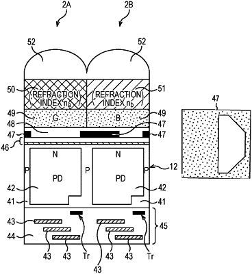
a first pixel including:
a first on-chip lens;
a first wiring layer;
a first photoelectric conversion region disposed between the first on-chip lens and the first wiring layer; and
a first color filter region disposed between the first on-chip lens and the first photoelectric conversion region in a cross-sectional view;
a second pixel adjacent to the first pixel, the second pixel including:
a second on-chip lens;
a second wiring layer;
a second photoelectric conversion region disposed between the second on-chip lens and the second wiring layer; and
a second color filter region disposed between the second on-chip lens and the second photoelectric conversion region in the cross-sectional view; and
a light shielding film disposed between the first on-chip lens and the first photoelectric conversion region and between the second on-chip lens and the second photoelectric conversion region, in the cross-sectional view,
wherein the light shielding film overlaps a first area of the first photoelectric conversion region and a second area of the second photoelectric conversion region,
wherein the second area is greater than the first area,
wherein light incident upon the light shielding film that overlaps with the second area of the second photoelectric conversion region forms at least two corner areas,
wherein a second aperture shape of the light shielding film that overlaps with the second area of the second photoelectric conversion region is a shape having at least two edges inset from the at least two corner areas, and
wherein the second aperture shape is a hexagonal shape, a semicircular shape or a triangular shape.
|