| CPC H01L 27/14603 (2013.01) [H01L 27/14612 (2013.01); H01L 27/1463 (2013.01)] | 20 Claims |

|
1. An image sensor comprising:
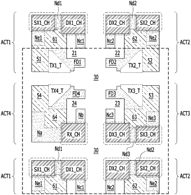
a first active region including a first floating diffusion region, a first transistor active region including a first drive transistor and a first select transistor, and a first isolation structure for electrically isolating the first floating diffusion region from the first transistor active region,
wherein the first isolation structure comprises a first P-typed doped region disposed on one corner of the first active region and a second P-typed doped region disposed in a center of the first active region, the first P-typed doped region and the second P-typed doped region being electrically coupled to each other and the first P-typed doped region including a contact structure configured to receive a ground voltage,
wherein the first active region further comprises a first transfer transistor region disposed between the first floating diffusion region and the first P-typed doped region, and
wherein a source region of the first select transistor is electrically isolated from the first transfer transistor region by the first P-typed doped region,
wherein a protruding portion of the first floating diffusion region abuts receding portions extended from the first isolation structure, and
wherein the receding portions extended from the first isolation structure include a first extension that is extended and disposed between the first floating diffusion region of the first active region and a drain region of the first drive transistor and between the first isolation structure and a drain region of the first drive transistor.
|