| CPC H01L 27/0886 (2013.01) [H01L 29/0673 (2013.01); H01L 29/0847 (2013.01); H01L 29/26 (2013.01); H01L 29/785 (2013.01)] | 20 Claims |

|
1. A method of manufacturing an integrated circuit device, the method comprising:
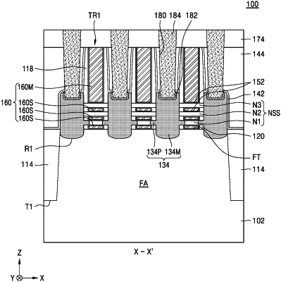
forming a structure including a fin-type active region and a pair of nanosheet stacks, the fin-type active region extending lengthwise in a first horizontal direction, each of the pair of nanosheet stacks including a plurality of nanosheets which overlap each other in a vertical direction on the fin-type active region;
partially removing a first nanosheet, which is closest to the fin-type active region from among the plurality of nanosheets of each of the pair of nanosheet stacks, to form a nanosheet indent region in each of the pair of nanosheet stacks; and
forming a source/drain region between the pair of nanosheet stacks on the fin-type active region, the source/drain region comprising a source/drain main region and a pair of source/drain protruding regions, wherein the source/drain main region is between the pair of nanosheet stacks, and the pair of source/drain protruding regions protrude in opposite directions from the source/drain main region toward the first nanosheet of each of the pair of nanosheet stacks and at least partially fill the nanosheet indent region in each of the pair of nanosheet stacks.
|