| CPC H01L 27/0605 (2013.01) [H01L 21/8258 (2013.01); H01L 27/0623 (2013.01); H01L 29/045 (2013.01); H01L 29/0649 (2013.01); H01L 29/16 (2013.01); H01L 29/2003 (2013.01)] | 20 Claims |

|
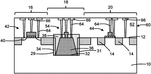
1. A structure comprising:
a bulk semiconductor substrate comprising a single-crystal semiconductor material having a <111>crystal orientation, the bulk semiconductor substrate having a first device region, and a second device region;
a bipolar junction transistor including a first terminal positioned in the single-crystal semiconductor material of the first device region of the bulk semiconductor substrate; and
a non-CMOS transistor in the second device region of the bulk semiconductor substrate, the non-CMOS transistor including a layer stack on the single-crystal semiconductor material of the bulk semiconductor substrate, and the layer stack including a layer comprising a III-V compound semiconductor material.
|