| CPC H01L 27/0605 (2013.01) [H01L 21/26546 (2013.01); H01L 21/266 (2013.01); H01L 21/30621 (2013.01); H01L 21/308 (2013.01); H01L 21/8252 (2013.01); H01L 27/0629 (2013.01); H01L 29/2003 (2013.01); H01L 29/205 (2013.01); H01L 29/66212 (2013.01); H01L 29/66462 (2013.01); H01L 29/7788 (2013.01); H01L 29/872 (2013.01)] | 21 Claims |

|
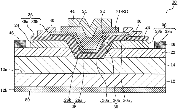
1. A nitride semiconductor device, comprising:
a substrate;
a first nitride semiconductor layer of a first conductivity disposed above the substrate;
a second nitride semiconductor layer of a second conductivity different from the first conductivity, disposed above the first nitride semiconductor layer;
a first opening penetrating through the second nitride semiconductor layer;
an electron transport layer and an electron supply layer disposed along inner surfaces of the first opening, the electron transport layer and electron supply layer being arranged in sequence from a substrate side such that the electron transport layer is closer to the substrate side and electron supply layer is further away from the substrate side;
a gate electrode disposed above the electron supply layer to cover the first opening;
a source electrode connected to the electron supply layer and the electron transport layer, at a position separated from the gate electrode; and
a drain electrode disposed on a surface of the substrate which is opposite to a surface on which the first nitride semiconductor layer is disposed,
wherein at least part of the second nitride semiconductor layer is fixed to a first potential that is different from a second potential applied to the source electrode.
|