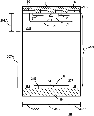
| CPC H01L 27/0262 (2013.01) [H01L 27/0928 (2013.01)] | 20 Claims |

|
1. A semiconductor device, comprising:
a region of semiconductor material comprising:
a top side;
a bottom side opposite to the top side;
a semiconductor substrate of a first conductivity type; and
a semiconductor region of the first conductivity type over the semiconductor substrate;
a well region of a second conductivity type opposite to the first conductivity type in the semiconductor region;
a first doped region of the first conductivity type in the well region;
a second doped region of the second conductivity type in the well region;
a third doped region of the second conductivity type in the semiconductor substrate at the bottom side;
a fourth doped region of the first conductivity type in the semiconductor substrate at the bottom side;
a first conductor coupled to the first doped region and the second doped region at the top side; and
a second conductor coupled to the third doped region and the fourth doped region at the bottom side;
wherein:
one or more of the third doped region or the fourth doped region is a patterned doped region; and
the semiconductor device is configured as a dual-sided semiconductor-controlled rectifier (SCR) device.
|