| CPC H01L 27/0248 (2013.01) [H01L 27/0255 (2013.01); H01L 27/0262 (2013.01); H01L 27/0292 (2013.01); H01L 27/0296 (2013.01)] | 19 Claims |

|
1. A transient voltage suppressing device, comprising:
an epitaxial layer on a surface of a substrate having a light concentration of ions of a first conductivity type wherein the first conductivity type is opposite a second conductivity type;
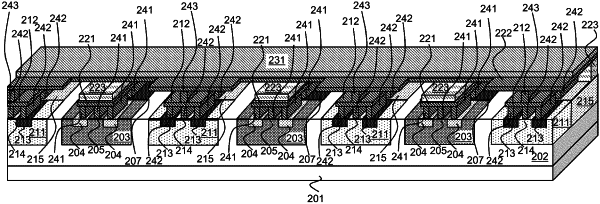
a plurality of fingers arranged laterally along a major surface of the epitaxial layer, the plurality of fingers comprising fingers of a first type and fingers of a second type, wherein the first type of finger and second type of finger each include a silicon controlled rectifier (SCR) portion and a junction diode portion, wherein the first type of finger includes a portion of a first metal layer that conductively couples the SCR portion to the junction diode portion, wherein the plurality of fingers of the second type are coupled together by a second metal layer electrically insulated from the first metal layer and disposed over top of the first metal layer, wherein a junction diode is formed between the junction diode portion of the first type of finger and the junction diode portion of the second type of finger; and wherein an SCR is formed between the SCR portion of the first type of finger and the SCR portion of the second type of finger wherein the fingers of the first type include a first well region lightly doped with ions of the first conductivity type formed in the epitaxial layer and a collector region heavily doped with ions of the second conductivity type formed in the first well region, wherein the first metal layer is conductively coupled to the collector region and connected by vias lined with conductive material to the first well region.
|