| CPC H01L 25/50 (2013.01) [H01L 25/167 (2013.01); H01L 27/15 (2013.01)] | 14 Claims |

|
1. A method of fabricating a hybrid element, the method comprising:
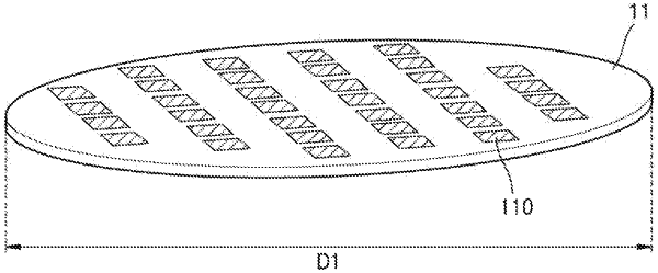
forming a plurality of first elements on a first substrate;
separating a plurality of second elements grown on a second substrate from the second substrate, a material of the second substrate being different from a material of the first substrate; and
transferring the plurality of second elements, separated from the second substrate, onto the first substrate,
wherein, in the transferring, the plurality of second elements are spaced apart from each other by a fluidic self-assembly method, and
wherein each of the plurality of second elements comprises a shuttle layer grown on the second substrate, an element layer grown on the shuttle layer, and an electrode layer on the element layer.
|