| CPC H01L 25/18 (2013.01) [G11C 16/08 (2013.01); G11C 16/24 (2013.01); H01L 24/20 (2013.01); H10B 41/10 (2023.02); H10B 41/27 (2023.02); H10B 41/35 (2023.02); H10B 41/41 (2023.02); H10B 43/10 (2023.02); H10B 43/27 (2023.02); H10B 43/35 (2023.02); H10B 43/40 (2023.02); H01L 2924/1431 (2013.01); H01L 2924/1438 (2013.01)] | 7 Claims |

|
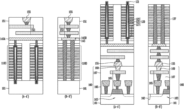
1. A method of manufacturing a semiconductor memory device, the method comprising:
forming a memory cell array on a sacrificial substrate, wherein the memory cell array includes:
interlayer insulating layers and conductive patterns, which are alternately stacked on the sacrificial substrate,
a channel structure penetrating the interlayer insulating layers and the conductive patterns, and
a memory layer extending along a surface of the channel structure;
removing the sacrificial substrate to expose the memory layer;
removing a portion of the memory layer to expose a first end portion of the channel structure; and
forming a common source line at a temperature of 450° C. or less, wherein the common source line is in direct contact with the first end portion of the channel structure and extends to overlap the memory cell array.
|