| CPC H01L 25/18 (2013.01) [H01L 24/32 (2013.01); H01L 24/83 (2013.01); H01L 2224/32145 (2013.01); H01L 2224/83896 (2013.01); H01L 2924/1431 (2013.01); H01L 2924/1437 (2013.01)] | 20 Claims |

|
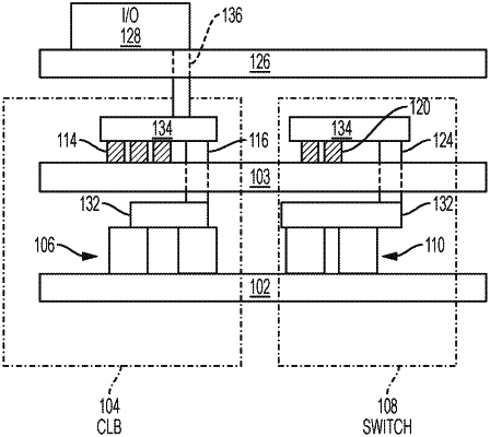
1. An integrated circuit including a field programmable gate array (FPGA) device, the integrated circuit comprising:
a first semiconductor substrate;
a second semiconductor substrate over the first semiconductor substrate;
a dielectric layer between the first semiconductor substrate and the second semiconductor substrate;
a configurable logic block (CLB) including a logic transistor between the first semiconductor substrate and the second semiconductor substrate, and a memory cell over the second semiconductor substrate; and
a via directly connecting the logic transistor and the memory cell, the via disposed entirely through the second semiconductor substrate and extending above an uppermost surface of the second semiconductor substrate, the via over and vertically overlapping with the logic transistor and beneath and vertically overlapping with the memory cell, and the via having a bottommost surface above an uppermost surface of the logic transistor.
|