| CPC H01L 25/167 (2013.01) [H01L 24/03 (2013.01); H01L 24/05 (2013.01); H01L 27/1259 (2013.01); H01L 33/42 (2013.01); H01L 2224/03622 (2013.01); H01L 2224/05018 (2013.01); H01L 2224/05076 (2013.01); H01L 2224/05084 (2013.01); H01L 2224/05166 (2013.01); H01L 2224/05186 (2013.01); H01L 2224/05558 (2013.01); H01L 2224/05573 (2013.01); H01L 2224/05686 (2013.01); H01L 2933/0016 (2013.01)] | 12 Claims |

|
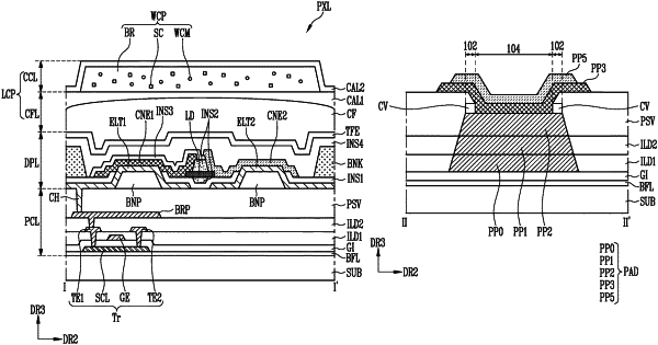
1. A display device having a pad area and a display area, the display device comprising:
a substrate;
a pad structure on a surface of the substrate in the pad area, the pad structure comprising a first pad pattern, a second pad pattern on an upper surface of the first pad pattern, and a third pad pattern on an upper surface of the second pad pattern; and
a display element part on the substrate in the display area, the display element part comprising a light emitting element configured to emit light in a display direction,
wherein the upper surface of the second pad pattern has a first area and a second area,
wherein the upper surface of the second pad pattern and the third pad pattern do not contact each other in the first area, and
wherein the upper surface of the second pad pattern and the third pad pattern contact each other in the second area.
|