| CPC H01L 25/105 (2013.01) [H01L 21/561 (2013.01); H01L 21/563 (2013.01); H01L 21/568 (2013.01); H01L 21/6835 (2013.01); H01L 21/76802 (2013.01); H01L 23/3121 (2013.01); H01L 23/3142 (2013.01); H01L 23/481 (2013.01); H01L 23/5389 (2013.01); H01L 24/05 (2013.01); H01L 24/19 (2013.01); H01L 24/20 (2013.01); H01L 24/24 (2013.01); H01L 24/96 (2013.01); H01L 24/97 (2013.01); H01L 25/50 (2013.01); H01L 23/3128 (2013.01); H01L 24/48 (2013.01); H01L 25/0657 (2013.01); H01L 2221/68345 (2013.01); H01L 2221/68359 (2013.01); H01L 2224/211 (2013.01); H01L 2224/24145 (2013.01); H01L 2224/48091 (2013.01); H01L 2224/48227 (2013.01); H01L 2225/0651 (2013.01); H01L 2225/06527 (2013.01); H01L 2225/06548 (2013.01); H01L 2225/06568 (2013.01); H01L 2225/06586 (2013.01); H01L 2225/1035 (2013.01); H01L 2225/1058 (2013.01); H01L 2924/00014 (2013.01); H01L 2924/1433 (2013.01); H01L 2924/1436 (2013.01); H01L 2924/181 (2013.01)] | 20 Claims |

|
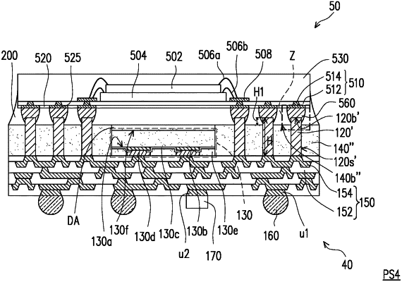
1. A method of manufacturing a package structure, comprising:
providing a first semiconductor die;
forming a plurality of conductive pillars next to the first semiconductor die;
encapsulating the first semiconductor die and the plurality of conductive pillars in a first encapsulant;
placing a redistribution circuit structure over the first semiconductor die and the plurality of conductive pillars;
disposing a plurality of contact pads over the redistribution circuit structure;
connecting the plurality of contact pads to the plurality of conductive pillars through a plurality of conductive connectors, wherein in a cross-section of the package structure, a lateral offset between a sidewall of one of the plurality of conductive pillars and a sidewall of a respective one of the plurality of conductive connectors is about 50 μm to about 100 μm;
disposing a second semiconductor die over the redistribution circuit structure; and
encapsulating the second semiconductor die in a second encapsulant.
|