| CPC H01L 25/105 (2013.01) [H01L 21/4853 (2013.01); H01L 21/4857 (2013.01); H01L 21/563 (2013.01); H01L 21/565 (2013.01); H01L 21/568 (2013.01); H01L 21/6835 (2013.01); H01L 23/3128 (2013.01); H01L 23/3135 (2013.01); H01L 23/5383 (2013.01); H01L 23/5386 (2013.01); H01L 23/5389 (2013.01); H01L 23/562 (2013.01); H01L 24/19 (2013.01); H01L 24/20 (2013.01); H01L 24/48 (2013.01); H01L 25/50 (2013.01); H01L 2221/68372 (2013.01); H01L 2224/214 (2013.01); H01L 2224/215 (2013.01); H01L 2224/48227 (2013.01); H01L 2225/1035 (2013.01); H01L 2225/1041 (2013.01); H01L 2225/1058 (2013.01); H01L 2924/01028 (2013.01); H01L 2924/01029 (2013.01); H01L 2924/01079 (2013.01); H01L 2924/3511 (2013.01)] | 19 Claims |

|
1. A semiconductor package device, comprising:
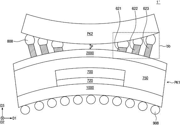
a redistribution substrate;
a first semiconductor package on the redistribution substrate; and
a plurality of first connection terminals between the redistribution substrate and the first semiconductor package,
wherein the redistribution substrate includes:
a dielectric layer;
a plurality of redistribution patterns which are vertically stacked in the dielectric layer and each of which includes a line part and a via part; and
a plurality of bonding pads on uppermost ones of the plurality of redistribution patterns,
wherein the plurality of bonding pads are exposed from the dielectric layer and are in contact with the first connection terminals,
wherein, when viewed in a plan view, the plurality of bonding pads are sized in decreasing diameters in a first direction from a central portion of a top surface of the redistribution substrate to an outer portion of the top surface of the redistribution substrate, and
wherein, when viewed in a cross-sectional view, the plurality of bonding pads are sized in increasing thicknesses in the first direction.
|