| CPC H01L 25/0753 (2013.01) [H01L 27/1225 (2013.01); H01L 29/78651 (2013.01); H01L 29/7869 (2013.01); H01L 33/504 (2013.01); H01L 33/58 (2013.01); H01L 33/62 (2013.01); H01L 2933/0041 (2013.01); H01L 2933/0058 (2013.01); H01L 2933/0066 (2013.01)] | 17 Claims |

|
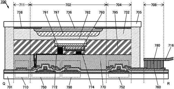
1. A display device comprising:
a first wiring;
a second wiring;
a third wiring;
a first transistor;
a second transistor;
a third transistor;
a capacitor;
a light-emitting element;
a coloring layer;
a first electrode;
a second electrode;
a first bump; and
a second bump,
wherein the light-emitting element is electrically connected to the first electrode and the second electrode,
wherein the first electrode is electrically connected to one of a source and a drain of the first transistor,
wherein the first electrode overlaps with a gate of the first transistor,
wherein the second electrode is positioned on the same plane as the first electrode,
wherein the coloring layer is positioned over the light-emitting element,
wherein the coloring layer includes a region overlapping with the light-emitting element,
wherein the light-emitting element includes a light-emitting diode chip,
wherein the light-emitting element is configured to emit white light,
wherein the first bump is positioned between one electrode of the light-emitting element and the first electrode,
wherein the second bump is positioned between the other electrode of the light-emitting element and the second electrode,
wherein one of a source and a drain of the second transistor is electrically connected to one electrode of the capacitor,
wherein one of a source and a drain of the third transistor is electrically connected to the other electrode of the capacitor,
wherein the one of the source and the drain of the third transistor is directly connected to the gate of the first transistor,
wherein a gate of the second transistor is electrically connected to the first wiring,
wherein a gate of the third transistor is electrically connected to the second wiring, and
wherein the other one of the source and the drain of the second transistor is electrically connected to the third wiring.
|