| CPC H01L 24/81 (2013.01) [H01L 24/11 (2013.01); H01L 24/13 (2013.01); H01L 24/14 (2013.01); H01L 24/16 (2013.01); H01L 2224/1146 (2013.01); H01L 2224/13083 (2013.01); H01L 2224/13147 (2013.01); H01L 2224/13155 (2013.01); H01L 2224/14132 (2013.01); H01L 2224/16148 (2013.01); H01L 2224/81125 (2013.01); H01L 2224/81193 (2013.01); H01L 2224/81815 (2013.01); H01L 2224/81908 (2013.01); H01L 2924/3511 (2013.01)] | 20 Claims |

|
1. A semiconductor package, comprising:
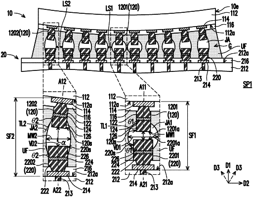
a first package component and a second package component stacked upon and electrically connected to each other, the first package component comprising a first conductive bump and a second conductive bump, the second package component comprising a third conductive bump and a fourth conductive bump, and dimensions of the first and second conductive bumps being less than dimensions of the third and fourth conductive bumps;
a first joint structure partially covering the first conductive bump of the first package component and the third conductive bump of the second package component; and
a second joint structure partially covering the second conductive bump of the first package component and the fourth conductive bump of the second package component, wherein a first angle between a sidewall of the first conductive bump and a tangent line at an end point of a boundary of the first joint structure on the sidewall of the first conductive bump is greater than a second angle between a sidewall of the second conductive bump and a tangent line at an end point of a boundary of the second joint structure on the sidewall of the second conductive bump.
|