| CPC H01L 24/32 (2013.01) [B23K 1/0016 (2013.01); H01L 24/83 (2013.01); H01L 29/41741 (2013.01); H01L 29/456 (2013.01); H01L 29/51 (2013.01); B23K 2101/40 (2018.08); H01L 2224/29083 (2013.01); H01L 2224/29166 (2013.01); H01L 2224/29184 (2013.01); H01L 2224/29205 (2013.01); H01L 2224/29209 (2013.01); H01L 2224/29211 (2013.01); H01L 2224/29213 (2013.01); H01L 2224/29217 (2013.01); H01L 2224/29218 (2013.01); H01L 2224/2922 (2013.01); H01L 2224/29239 (2013.01); H01L 2224/29244 (2013.01); H01L 2224/29247 (2013.01); H01L 2224/32227 (2013.01); H01L 2224/32245 (2013.01); H01L 2224/32503 (2013.01); H01L 2224/83201 (2013.01); H01L 2224/83203 (2013.01); H01L 2224/8321 (2013.01); H01L 2224/8381 (2013.01); H01L 2224/8382 (2013.01)] | 10 Claims |

|
1. A semiconductor assembly, comprising:
a substrate comprising a metal die attach surface;
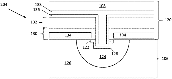
a semiconductor die that is arranged on the substrate, the semiconductor die being configured as a power semiconductor device and comprising a semiconductor body, a rear side metallization, and a front side layer stack, the front side layer stack comprising a front side metallization and a contaminant protection layer that is between the front side metallization and the semiconductor body; and
a diffusion soldered joint between the metal die attach surface and the rear side metallization, the diffusion soldered joint comprising one or more intermetallic phases throughout the diffusion soldered joint,
wherein the contaminant protection layer is configured to prevent transmission of contaminants into the semiconductor body.
|