| CPC H01L 23/66 (2013.01) [H01L 21/28575 (2013.01); H01L 21/8252 (2013.01); H01L 23/481 (2013.01); H01L 27/0605 (2013.01); H01L 27/0629 (2013.01); H01L 28/60 (2013.01); H01L 29/2003 (2013.01); H01L 29/205 (2013.01); H01L 29/452 (2013.01); H01L 29/66462 (2013.01); H01L 29/7786 (2013.01); H01L 23/53214 (2013.01); H01L 29/4175 (2013.01); H01L 2223/6616 (2013.01); H01L 2223/6683 (2013.01); H01L 2924/1423 (2013.01)] | 20 Claims |

|
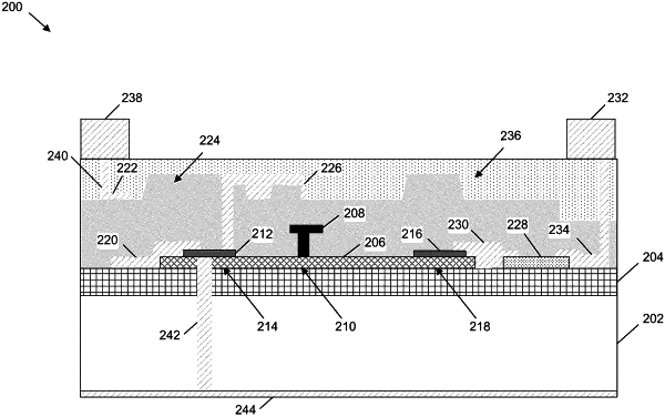
1. A device having a monolithic microwave integrated circuit comprises:
a substrate having:
a barrier layer disposed on the substrate, the barrier layer including an aluminum gallium nitride (AlGaN) material and including a drain region, a source region, and a gate region; and
a channel layer disposed between a surface of the substrate and the barrier layer, the channel layer including a gallium nitride (GaN) material;
a gate electrical contact disposed on the gate region of the barrier layer, the gate electrical contact including one or more non-gold-based metallic materials;
a source electrical contact disposed on the source region of the barrier layer, the source electrical contact including a non-gold-based metallic material of the one or more non-gold-based metallic materials;
a drain electrical contact disposed on the drain region of the barrier layer, the drain electrical contact including the non-gold-based metallic material of the one or more non-gold-based metallic materials; and
a capacitor including a first plate, a second plate, and a dielectric material disposed between the first plate and the second plate, wherein at least a portion of the first plate is disposed on at least one of the channel layer or the barrier layer; the second plate is disposed on the dielectric material; and the first plate and the second plate include the non-gold-based metallic material of the one or more non-gold-based metallic materials.
|