| CPC H01L 23/5389 (2013.01) [H01L 21/4857 (2013.01); H01L 21/565 (2013.01); H01L 23/3121 (2013.01); H01L 23/5383 (2013.01); H01L 23/5384 (2013.01); H01L 23/5386 (2013.01); H01L 25/0652 (2013.01); H01L 23/5221 (2013.01); H01L 23/5381 (2013.01); H01L 24/16 (2013.01); H01L 2224/023 (2013.01); H01L 2224/0233 (2013.01); H01L 2224/16235 (2013.01)] | 20 Claims |

|
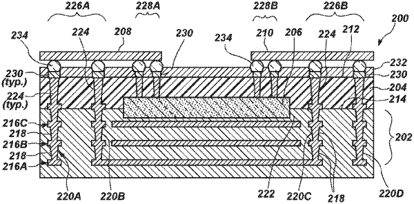
1. A method of forming an embedded die package, comprising:
forming a substrate, the substrate defining multiple layers of conductive traces separated by respective layers of dielectric material;
placing an embedded die on a receiving surface of the substrate;
forming a molded component extending over a surface of the substrate and over at least a portion of the embedded die, the molded component formed with a planar outer surface independent of undulations at the surface of the substrate; and
forming multiple vertical contacts including:
a first group of vertical contacts extending though the molded component and arranged at a first pitch with respect to one another; and
a second group of contacts extending through the molded component and arranged at a second pitch with respect to one another, the second pitch smaller than the first pitch.
|