| CPC H01L 23/5384 (2013.01) [H01L 21/486 (2013.01); H01L 21/50 (2013.01); H01L 21/76802 (2013.01); H01L 21/76877 (2013.01); H01L 23/5386 (2013.01); H01L 25/0657 (2013.01)] | 20 Claims |

|
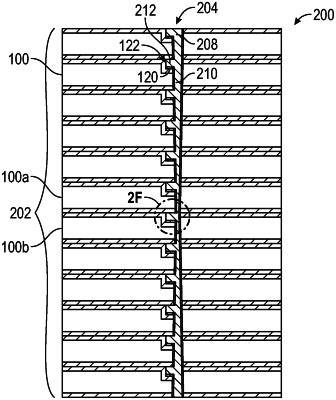
19. A method of forming a semiconductor assembly, the method comprising:
assembling a die stack including a plurality of semiconductor dies, wherein each semiconductor die includes:
a first surface including a first insulating material,
a second surface opposite the first surface, the second surface including a second insulating material,
a recess in the first surface, and
a conductive pad within the recess,
wherein neighboring semiconductor dies in the die stack are directly coupled to each other via the respective first and second insulating materials of the neighboring semiconductor dies; and
electrically coupling a conductive structure to each of the plurality of semiconductor dies, wherein the conductive structure includes:
a monolithic via extending through each of the semiconductor dies in the die stack, and
a plurality of protrusions extending laterally from the monolithic via, wherein the plurality of protrusions and the monolithic via are made of a continuous material, and wherein each protrusion is positioned within the recess of a respective one of the semiconductor dies and is electrically coupled to the conductive pad within the recess.
|